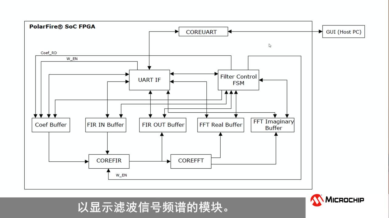
|
Altera公司的Stratix V FPGA包括GT, GX, GS和E四個系列,采用28nm技術,集成了高達28.05Gbps的收發器和獨特的硬件IP區塊,適合不同的應用如包括PCI Express® (PCIe®)Gen3在內的寬帶應用,40G/100G和更高的數據應用,高性能高精度的DSP應用.本文介紹了Stratix V FPGA主要特性,Stratix V GT, GX和GS 器件框圖以及Altera® Stratix® V GX FPGA開發套件主要特性和元件區塊,框圖,Stratix V GX FPGA開發板主要元件表,電路圖和材料清單,PCB布局圖. Altera’s 28-nm Stratix V FPGAs include innovations such as an enhanced core architecture, integrated transceivers up to 28.05 gigabits per second (Gbps), and a unique array of integrated hard intellectual property (IP) blocks. With these innovations, Stratix V FPGAs deliver a new class of application-targeted devices optimized for: ■ Bandwidth-centric applications and protocols, including PCI Express® (PCIe®)Gen3 ■ Data-intensive applications for 40G/100G and beyond ■ High-performance, high-precision digital signal processing (DSP) applications Stratix V devices are available in four variants (GT, GX, GS, and E), each targeted for a different set of applications. For higher volume production, you can prototype with Stratix V FPGAs and use the low-risk, low-cost path to HardCopy® V ASICs. Stratix V GT devices, with both 28.05-Gbps and 12.5-Gbps transceivers, are optimized for applications that require ultra-high bandwidth and performance in areas such as 40G/100G/400G optical communications systems and optical test systems. 28.05-Gbps and 12.5-Gbps transceivers are also known as GT and GX channels, respectively. Stratix V GX devices offer up to 66 integrated 14.1-Gbps transceivers supporting backplanes and optical modules. These devices are optimized for high-performance, high-bandwidth applications such as 40G/100G optical transport, packet processing,and traffic management found in wireline, military communications, and network test equipment markets. Stratix V GS devices have an abundance of variable precision DSP blocks, supporting up to 3,926 18x18 or 1,963 27x27 multipliers. In addition, Stratix V GS devices offer integrated 14.1-Gbps transceivers, which support backplanes and optical modules. These devices are optimized for transceiver-based DSP-centric applications found in wireline, military, broadcast, and high-performance computing markets. Stratix V E devices offer the highest logic density within the Stratix V family with nearly one million logic elements (LEs) in the largest device. These devices are optimized for applications such as ASIC and system emulation, diagnostic imaging, and instrumentation. Stratix V FPGA主要特性: ■ Technology ■ 28-nm TSMC process technology ■ 0.85-V core voltage ■ Low-power serial transceivers ■ 28.05-Gbps transceivers on Stratix V GT devices ■ Electronic dispersion compensation (EDC) for XFP, SFP+, QSFP, CFP optical module support ■ Adaptive linear and decision feedback equalization ■ 600-Megabits per second (Mbps) to 14.1-Gbps backplane capability ■ Transmit pre-emphasis and de-emphasis ■ Dynamic reconfiguration of individual channels ■ On-chip instrumentation (EyeQ non-intrusive data eye monitoring) ■ General-purpose I/Os (GPIOs) ■ 1.4-Gbps LVDS ■ 1,066-MHz external memory interface ■ On-chip termination (OCT) ■ 1.2-V to 3.3-V interfacing for all Stratix V devices ■ Embedded HardCopy Block ■ PCIe Gen3, Gen2, and Gen1 complete protocol stack, x1/x2/x4/x8 end point and root port ■ Embedded transceiver hard IP ■ Interlaken physical coding sublayer (PCS) ■ Gigabit Ethernet (GbE) and XAUI PCS ■ 10G Ethernet PCS ■ Serial RapidIO® (SRIO) PCS ■ Common Public Radio Interface (CPRI) PCS ■ Gigabit Passive Optical Networking (GPON) PCS ■ Power Management ■ Programmable Power Technology ■ Quartus II integrated PowerPlay Power Analysis ■ High-performance core fabric ■ Enhanced ALM with four registers ■ Improved routing architecture reduces congestion and improves compile times ■ Embedded memory blocks ■ M20K: 20-Kbit with hard error correction code (ECC) ■ MLAB: 640-bit ■ Variable precision DSP blocks ■ Up to 500 MHz performance ■ Natively support signal processing with precision ranging from 9x9 up to 54x54 ■ New native 27x27 multiply mode ■ 64-bit accumulator and cascade for systolic finite impulse responses (FIRs) ■ Embedded internal coefficient memory ■ Pre-adder/subtractor improves efficiency ■ Increased number of outputs allows more independent multipliers ■ Fractional PLLs ■ Fractional mode with third-order delta-sigma modulation ■ Integer mode ■ Precision clock synthesis, clock delay compensation, and zero delay buffer (ZDB) ■ Clock networks ■ 717-MHz fabric clocking ■ Global, quadrant, and peripheral clock networks ■ Unused clock networks can be powered down to reduce dynamic power ■ Device Configuration ■ Serial and parallel flash interface ■ Enhanced advanced encryption standard (AES) design security features ■ Tamper protection ■ Partial and dynamic reconfiguration ■ Configuration via Protocol (CvP) ■ High-performance packaging ■ Multiple device densities with identical package footprints enables seamless migration between different FPGA densities ■ FBGA packaging with on-package decoupling capacitors ■ Lead and RoHS-compliant lead-free options ■ HardCopy V migration 
圖1.Stratix V GT, GX和GS 器件框圖 Altera® Stratix® V GX FPGA開發套件 The Altera® Stratix® V GX FPGA Development Kit is a complete design environment that includes both the hardware and software you need to develop Stratix V GX FPGA designs. The following list describes what you can accomplish with the kit: ■ Test signal quality of the FPGA transceiver I/Os (up to 12.5 Gbps). ■ Develop and test PCI Express® (PCIe) 2.0 designs. ■ Develop and test memory subsystems consisting of SyncFlash, DDR3, and QDRII+. ■ Develop and test SDI with the embedded 75-ohm 3G SDI transceivers. ■ Develop embedded designs utilizing the Nios® II processor and external memory. ■ Develop and test network designs utilizing Triple Speed Ethernet MegaCore® and external RJ-45 jack. ■ Develop and test optical networking designs using the 10G and 40G Ethernet MAC MegaCores and the QSFP Optical Interface. ■ Take advantage of the modular and scalable design by using the high-speed mezzanine card (HSMC) connectors to interface to over 40 different HSMCs provided by Altera partners, supporting protocols such as Serial RapidIO®, 10 Gigabit Ethernet, SONET, Common Public Radio Interface (CPRI), Open Base Station Architecture Initiative (OBSAI) and others. ■ Measure the FPGA’s power consumption. ■ Control twelve different programmable clock oscillators using the Clock Control GUI.The Stratix V GX FPGA Development Kit includes the following hardware: ■ Stratix V GX FPGA development board—A development platform that allows you to develop and prototype hardware designs running on the Stratix V GX FPGA. ■ HSMC loopback board—A daughtercard that allows for loopback testing all signals on the HSMC interface using the Board Test System. ■ Power supply and cables—The kit includes the following items: ■ Power supply and AC adapters for North America/Japan, Europe, and the United Kingdom ■ Standard USB A to micro-USB cable ■ Ethernet cable ■ 75 Ω SMB video cable 軟件包括: The Quartus II Development Kit Edition (DKE) software includes the following items: ■ Quartus II Software—The Quartus II software, including the Qsys system integration tool, provides a comprehensive environment for network on a chip (NoC) design. The Quartus II software integrates into nearly any design environment and provides interfaces to industry-standard EDA tools. ■ MegaCore® IP Library—A library that contains Altera IP MegaCore functions. You can evaluate MegaCore functions by using the OpenCore Plus feature to do the following: ■ Simulate behavior of a MegaCore function within your system. ■ Verify functionality of your design, and quickly and easily evaluate its size and speed. ■ Generate time-limited device programming files for designs that include MegaCore functions. ■ Program a device and verify your design in hardware Altera® Stratix® V GX FPGA開發板包括以下主要的元件區塊: ■ Altera Stratix V FPGA (5SGXEA7K2F40C2) in the 1517-pin FineLine BGA Package ■ 622,000 Les ■ 358,500 adaptive logic modules (ALMs) ■ 50-Mbits embedded memory ■ 36 transceivers (12.5 Gbps) ■ 174 full-duplex LVDS channels ■ 28 phase locked loops (PLLs) ■ 512 18x18-bit multipliers ■ 850-mV core voltage ■ 696 user I/Os ■ 2 PCI Express hard IP blocks ■ MAX® V CPLD (5M2210ZF256C4) System Controller in the 256-pin FineLine BGA Package ■ 2,210 Les ■ 203 user I/Os ■ 1.8-V core voltage ■ FPGA Configuration Circuitry ■ MAX II CPLD (EPM570GM100) and Flash Fast Passive Parallel (FPP) configuration ■ On-Board USB-BlasterTM II for use with the Quartus® II Programmer, Nios® II Software Build Tools, and System Console. ■ On-Board Clocking Circuitry ■ 50-MHz, 100-MHz, 125-MHz, and programmable oscillators ■ SMA connector for clock input (LVPECL) ■ Memory devices ■ 1152-Mbyte DDR3 SDRAM with a 72-bit data bus ■ 4.5-Mbyte QDRII+ SRAM with a 18-bit data bus (footprint is compatible for 9-Mbyte QDRII with a 18-bit data bus) ■ Two 512-Mbyte synchronous flash with a 16-bit data bus ■ Communication Ports ■ PCI Express (PCIe) x8 edge connector ■ Two HSMC ports ■ One universal HSMC port A ■ One DQS-type HSMC port B ■ SMB for SDI input and output ■ QSFP ■ USB 2.0 ■ Gigabit Ethernet ■ LCD header ■ General User I/O ■ 16 user LEDs ■ Two-line character LCD display ■ Six configuration status LEDs ■ Five PCI Express LEDs ■ Four Ethernet LEDs ■ Push Button and DIP Switches ■ One CPU reset push button ■ Three general user push buttons ■ Two configuration push buttons ■ Eight user DIP switches ■ Four MAX V control DIP switches ■ Power ■ 19-V (laptop) DC input ■ PCI Express edge connector power ■ On-Board power measurement circuitry ■ System Monitoring ■ Power—voltage, current, wattage ■ Temperature—FPGA die, local board ■ Mechanical ■ PCI Express short form factor ■ PCI Express chassis or bench-top operation
圖2.Stratix V GX FPGA開發板框圖
圖3.Stratix V GX FPGA開發板外形和特性圖 Stratix V GX FPGA開發板主要元件表:
圖4.Stratix V GX FPGA開發板電路圖(1) 更詳細的Stratix V GX FPGA開發板電路圖詳見:  Stratix V GX FPGA開發板材料清單.rar
(22.45 KB)
Stratix V GX FPGA開發板材料清單.rar
(22.45 KB)
Stratix V GX FPGA開發板材料清單見:
圖5.Stratix V GX FPGA開發板PCB元件布局圖:正面
圖6.Stratix V GX FPGA開發板PCB元件布局圖:背面
20120517113231925.rar
(1.51 MB)
 stx5_51001.pdf
(388.27 KB)
stratixvgx_5sgxea7kf40es_fpga_v11.1.2.part01.rar
(30 MB)
stratixvgx_5sgxea7kf40es_fpga_v11.1.2.part02.rar
(30 MB)
stratixvgx_5sgxea7kf40es_fpga_v11.1.2.part03.rar
(30 MB)
stratixvgx_5sgxea7kf40es_fpga_v11.1.2.part04.rar
(30 MB)
stratixvgx_5sgxea7kf40es_fpga_v11.1.2.part05.rar
(30 MB)
stratixvgx_5sgxea7kf40es_fpga_v11.1.2.part06.rar
(30 MB)
stratixvgx_5sgxea7kf40es_fpga_v11.1.2.part07.rar
(30 MB)
stratixvgx_5sgxea7kf40es_fpga_v11.1.2.part08.rar
(9.76 MB)
stx5_51001.pdf
(388.27 KB)
stratixvgx_5sgxea7kf40es_fpga_v11.1.2.part01.rar
(30 MB)
stratixvgx_5sgxea7kf40es_fpga_v11.1.2.part02.rar
(30 MB)
stratixvgx_5sgxea7kf40es_fpga_v11.1.2.part03.rar
(30 MB)
stratixvgx_5sgxea7kf40es_fpga_v11.1.2.part04.rar
(30 MB)
stratixvgx_5sgxea7kf40es_fpga_v11.1.2.part05.rar
(30 MB)
stratixvgx_5sgxea7kf40es_fpga_v11.1.2.part06.rar
(30 MB)
stratixvgx_5sgxea7kf40es_fpga_v11.1.2.part07.rar
(30 MB)
stratixvgx_5sgxea7kf40es_fpga_v11.1.2.part08.rar
(9.76 MB)
來源:網絡 |